

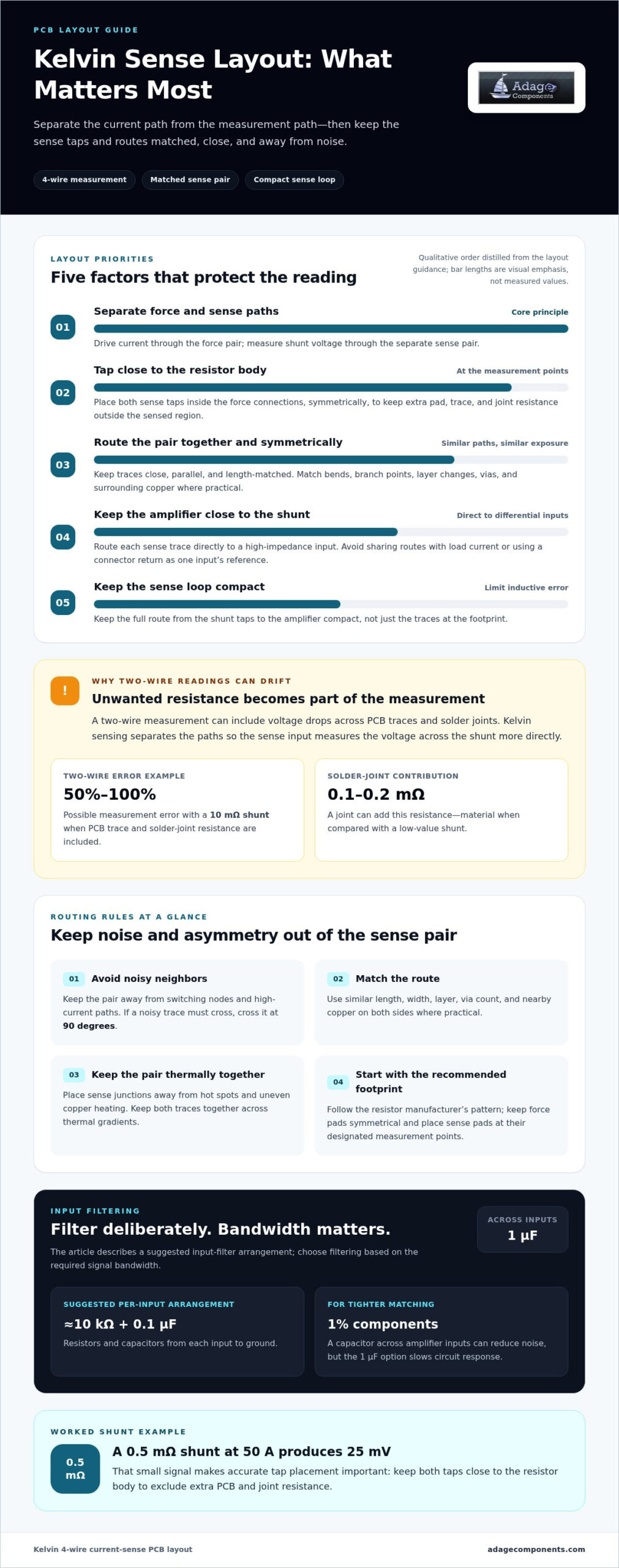
For accurate Kelvin sensing, use two force pads and two sense pads, with the sense taps placed close to the resistor body inside the force connections. The essential Kelvin 4-wire current sense PCB pad layout best practices are to route the sense lines as a short, closely spaced pair, away from high-current paths and switching noise.
A two-wire measurement can include voltage drops across PCB traces and solder joints, distorting the shunt reading. A Kelvin connection separates the current path from the voltage-measurement path, so the sense input measures the voltage across the shunt more directly.
This guide covers shunt pad placement, separate force and sense routing, noise reduction, and ways to limit inductive error by keeping the sense loop compact. It also explains when PCB Kelvin taps on a two-pad shunt may be suitable and how a true four-terminal shunt differs.
Key Takeaways
- Separate force and sense connections so the measurement captures the shunt’s voltage drop rather than unwanted PCB resistance.
- Place sense taps close to the resistor body and route the pair together, away from switching nodes and high-current paths.
- Choose between PCB Kelvin taps and a true four-terminal shunt based on how much connection resistance your measurement can tolerate.
- Keep the sense loop compact and position the amplifier close to the shunt to help limit inductive error.
- Start the footprint with the resistor manufacturer’s recommended pattern, then preserve symmetrical force pads and sense connections in the layout.
What is the Purpose of the Kelvin Connection?
- Separate the current path from the voltage-measurement path. A Kelvin 4-wire connection drives current through one pair of terminals and measures voltage across a second pair. Ideally, negligible current flows through the sense conductors, apart from leakage and input bias currents. This prevents force-lead voltage drops from becoming part of the shunt measurement.
- Estimate two-wire error before selecting a layout. With a 10 mΩ shunt, PCB trace and solder-joint resistance can cause a 50% to 100% measurement error. A solder joint can add 0.1-0.2 mΩ, which becomes material when compared with a low-value shunt. Even a few tenths of a milliohm in joints and traces can create an error of 20% or more in a two-wire measurement.
- Place the sense taps at the resistor’s measurement points, not at remote connector terminals. The shunt produces a voltage drop proportional to current, so extra resistance between the tap and resistor changes the voltage being measured. For example, a 0.5 mΩ shunt carrying 50 A produces 25 mV. Keep both sense taps symmetrical and close to the resistor body to exclude more PCB and joint resistance.
- Account for copper pours, vias, and solder in the force path. Copper pours and vias can reduce force-path resistance when sized and connected for the current, but their resistance still contributes to voltage drop outside the sensed region. A 1 oz copper trace, 1 mm wide and 10 mm long, has roughly 5 mΩ resistance. Solder and pad interfaces add resistance too, so keep their effects outside the sense points where possible.
- Set current and temperature limits from shunt dissipation and resistance drift. Calculate shunt heating from I²R at maximum operating current, then select a power rating with margin. Copper resistance changes by roughly +3900 ppm/°C, while shunt TCR varies by resistor technology. Typical values are ±100 to ±200 ppm/°C for standard thick-film resistors, ±50 to ±75 ppm/°C for metal-strip current-sense resistors, and ±5 to ±15 ppm/°C for precision metal-foil shunts.
- Verify the assembled board across its approved operating range. Measure the shunt voltage at 10%, 50%, and 100% of approved operating current, then compare readings against the expected current-to-voltage relationship. For highest accuracy, calibrate the assembled Kelvin-sensing design and account for the shunt’s temperature coefficient. Record readings after the shunt reaches operating temperature, because heating changes resistance and can shift the result.
Sense-pair routing and noise reduction
Build the sense route as a matched path from the resistor’s measurement points to the amplifier. Apply Kelvin 4-wire current sense PCB pad layout best practices across the full route, including layer changes and nearby copper, not only at the shunt footprint.
-
Route the Sense Pair Differentially
Run positive and negative sense traces close together, parallel, and length-matched from their shunt taps. This arrangement helps both conductors experience similar electromagnetic interference, which a differential amplifier can reject. Keep the pair clear of switching nodes and high-current paths; if a noisy trace must cross, cross it at 90 degrees.
Keep bends and branch points consistent on both sides. If the pair changes layers, transition both traces together with nearby vias, then continue along comparable paths. A detour on only one input changes its exposure to nearby signals. These Kelvin 4-wire current sense PCB pad layout best practices also make layout reviews easier because asymmetrical routing stands out.
-
Keep Sense Routes Symmetrical
Tap each sense trace from the corresponding inner point of its resistor pad, then route both toward the amplifier using similar geometry. Match route length, width, layer, and surrounding copper where practical. Differences between the paths can create unequal resistance and noise pickup at the amplifier inputs.
Keep the two sense junctions at similar temperatures. Place them away from hot spots, power components, and areas of uneven copper heating, which can create thermoelectric voltage errors. If the routes cross a thermal gradient, keep them together through that area rather than routing them along separate paths.
-
Connect Sense Traces to the Amplifier
Route the pair directly to the current-sense amplifier’s differential inputs, and place the amplifier close to the shunt. Connect each trace to a high-impedance input so negligible current flows through the sense wiring. Don’t share a route with load-current connections or use a connector return as the reference for one input.
For input filtering, one suggested arrangement uses approximately 10 kΩ resistors and 0.1 µF capacitors from each input to ground. Match components to 1% when tighter matching is desired. A 1 µF capacitor across the amplifier inputs can reduce noise, but it slows circuit response. Select filtering based on the required signal bandwidth.
-
Plan Pads and Traces for Sensing
Start with the resistor manufacturer’s recommended footprint. Keep the force pads symmetrical in size and copper connection, then place each sense pad at its designated measurement point. Don’t extend one sense connection into the force path or let a copper pour shift one tap relative to the other.
Review the complete route from the shunt pads to the amplifier. Look for parallel runs beside switching nets, unequal via counts, and different nearby copper on either side. Applying Kelvin 4-wire current sense PCB pad layout best practices to these footprint and routing checks helps maintain a consistent measurement path. Compare component options with the layout requirements before finalizing the design.
Four-terminal versus two-terminal shunts
Choose the shunt terminal arrangement according to where its voltage-measurement points are defined. Because pad dimensions vary by resistor, use the manufacturer-specified footprint rather than a generic pattern.
- Check whether the resistor has a true internal Kelvin connection. A four-terminal shunt separates its current-carrying terminals from its voltage-measurement terminals inside the component. The manufacturer defines these internal connection points, so the PCB can route force and sense connections to their designated terminals without relying on board copper to define the measurement points.
- PCB Kelvin taps can be used with a two-terminal shunt when its construction and the required accuracy suit the design. A regular two-pad footprint may work, with sense traces tapped as close as practical to the resistor body. This excludes voltage drops along the high-current PCB traces, but the measurement still includes effects from the pad-to-resistor interface, solder, and connection surfaces.
- Read the package drawing before setting pad dimensions or spacing. Follow the resistor manufacturer’s recommended footprint, including terminal placement and solder-land geometry. Keep the force pads equal in size and copper connection to support balanced reflow. Position sense taps at corresponding inner points without extending them into the force path or changing the intended measurement location.
- Don’t assume every four-pad land pattern is for a true four-terminal shunt. Some two-terminal resistors use physically split pads, with separate sections for current and voltage traces. Those extra PCB pads don’t necessarily provide an internal Kelvin connection; the sensed voltage can still include resistance from solder and the resistor’s external connection surfaces. Confirm the component’s terminal construction in its datasheet and drawing.
- Match the topology to the measurement error budget. A forum discussion uses 1% as an illustrative, approximate accuracy level where a two-pad resistor with PCB Kelvin taps may suffice. It suggests a four-pad resistor for an illustrative, approximate 0,01% accuracy level. Treat these as examples, not universal thresholds; shunt construction, assembly interfaces, temperature, and the complete measurement circuit all affect accuracy.
- For a removable Kelvin test setup, use a four-terminal connector to keep force and measurement leads separate. Label the current and voltage terminals clearly in the schematic and silkscreen. Before release, compare the PCB footprint with the exact component drawing and trace each sense net to its assigned measurement terminal.
Use the resistor manufacturer’s package drawing and recommended footprint for pad dimensions, spacing, and solder-land geometry. Keep the force pads matched in size and copper connection, and place sense connections at corresponding inner points without extending them into the force path.
Four-wire force and sense path separation
Connect each Kelvin sense trace to its matching shunt terminal at the inner, symmetrical point, close to the resistor body. Reserve the two force connections for load current, and route the two sense connections independently to high-impedance inputs.
- Assign four separate nets before routing: force positive, force negative, sense positive, and sense negative. The force pair carries load current through the shunt; the sense pair measures voltage. Keeping the nets distinct in the schematic and PCB layout helps reveal accidental connections that could divert current through a sense trace.
- Place sense taps directly at the shunt’s voltage-measurement terminals. For a two-terminal part with PCB Kelvin taps, use corresponding inner points on the pads, close to the resistor body. For a true four-terminal shunt, route from its dedicated voltage terminals. In either case, don’t tap at a distant connector or along a high-current trace.
- Route each force net through its own large pad and into the load-current path. Keep the force pads symmetrical in size and copper connection so their solder joints and heat flow remain balanced. Don’t use a sense pad, narrow branch, or amplifier input trace as a parallel route for shunt current.
- Keep the sense nets outside the force-current path from their taps to the amplifier. Connect them to high-impedance inputs so negligible current flows through the conductors. This keeps sense wiring from becoming an unintended current path, where even a few milliohms can shift the measured voltage.
- Inspect copper pours and plane connections around all four terminals. A pour that bridges a force pad to a sense pad can create a parallel path and change the effective measurement points. Preserve the intended separation on every copper layer, and review thermal reliefs, vias, and plane clearances around the shunt footprint.
- Trace all four nets through the finished layout before release. Confirm that both force nets connect to the load path and both sense nets connect only to their intended measurement terminals and amplifier inputs. Review the schematic, footprint, and PCB together: a four-pad pattern alone doesn’t prove that the resistor has an internal Kelvin connection.
A Kelvin shunt layout should use two large force pads and two smaller sense pads in a dedicated four-pad pattern. Match the pad pattern to the intended force and sense assignments, and verify the actual terminal connections rather than relying on pad shape alone. Route PCB current-sense lines directly to the shunt-resistor terminals, with connections as close as possible to the resistor body. This limits voltage-drop errors associated with the PCB layout and keeps the measurement reference at the shunt.
The layout should prevent load current from finding unintended paths through the measurement connections. Even a few milliohms can cause measurement errors, so inspect the copper around the shunt and keep the force and sense pads’ roles distinct. Check that the geometry and routing preserve this separation from the shunt terminals to the measurement circuitry.
Inductive error and sense-loop area
An enlarged sense loop or exposure to switching fields can add inductive voltage to the shunt reading. Keep the sense pair compact, route it away from noisy conductors, and place the amplifier near the shunt.
- Minimize the area enclosed by the positive and negative sense routes. Route them together from the shunt to the amplifier instead of taking separate paths around components or board edges. A changing magnetic field couples more readily into a large loop, creating voltage that can appear as measurement error during fast current changes.
- Keep the sense pair away from switching nodes and high-current paths. A nearby power trace can generate a changing magnetic field, while a long parallel run increases unwanted coupling. If a crossing is unavoidable, cross the noisy trace at 90 degrees and resume the paired route immediately afterward.
- Place the sense amplifier close to the shunt. This shortens the sensitive input path and limits the distance over which external fields can couple into the measurement. Route the amplifier inputs as a tight pair right up to their pins, and avoid branches that add loop area.
- Select a shunt designed for low equivalent series inductance when high-frequency accuracy matters. Metal-strip current-sense resistors designed for low ESL are usually less than 1 nH. Their internal construction can reduce inductive contribution, but PCB routing still matters: a low-ESL component cannot remove interference picked up by a broad external sense loop.
- Inspect every layer for routes that separate the sense conductors. A layer change can widen the loop if only one signal uses a via or the return path detours. Keep transitions adjacent, maintain close spacing between the pair, and don’t route one input over a switching region while the other follows a quieter path.
- Use a guard trace or shielding only when the board environment requires it. A guard can help protect sensitive traces, but it must not carry load current or create an unintended connection to either sense input. Review the copper around the shunt and amplifier together, then compare the layout with the selected current-sensing resistor options before finalizing component placement.
- Validate the layout under the circuit’s actual switching conditions. Compare the sensed signal with switching activity, and look for spikes that change when the sense-loop geometry changes. This helps distinguish inductive pickup from steady shunt drop and guides layout revisions toward the source of the error.
Judge layout choices against the observed response, not appearance alone. During the final review, check that the sense amplifier is close to the shunt and that the paired route stays compact all the way to its pins. If changing the geometry alters the spikes, revisit the routes and transitions around the shunt before accepting the layout. Keep the review focused on the sensitive measurement path and its enclosed area.
Adage Components: Thick Film Chip Resistors
Adage Components offers Thick Film Chip Resistors for OEM and EMS requirements. We also supply Thin Film Precision Resistors, Carbon Film Resistors, and MELF Resistors. Our direct, verified procurement channels support cost-effective sourcing of authentic components, with manufacturer pricing for your component requirements.
We support international logistics and work to provide shorter-than-average lead times. To select a resistor, align its specifications with your design and procurement requirements, then review the available options through our resistor linecard.
Contact Adage Components to discuss your sourcing requirements.
Carry the Layout into Component Selection
Use the design handoff to keep the PCB footprint, resistor specification, and bill of materials aligned. Applying Kelvin 4-wire current sense PCB pad layout best practices is most effective when the selected component’s terminal arrangement and electrical characteristics match the measurement approach. Resolve that alignment before the design is released, so sourcing decisions support the intended layout rather than forcing late footprint changes.
Adage Components supplies Thick Film Chip Resistors, Thin Film Precision Resistors, and Carbon Film Resistors. Compare the component options with your design criteria and approved parts list, then submit your RFQ or BOM to discuss your sourcing requirements.
Review Adage Components’ resistor linecard to support your component-selection process. A disciplined match between the design and the selected part helps keep your next engineering handoff clear and actionable.
Frequently Asked Questions
What is a Kelvin Resistor?
A Kelvin resistor is measured using separate force and sense connections instead of measuring through the same two terminals. The term describes the measurement arrangement, not a distinct resistor material. In a PCB design, check the component drawing: a genuine four-terminal shunt has separate current and voltage terminals, while a split-pad footprint alone doesn’t establish an internal Kelvin connection.
How should force and sense traces be routed to minimize measurement error?
Route force traces to carry load current through the shunt, and connect sense traces only to the designated voltage-measurement points. During bench validation, keep those connections separate in the test fixture too: use four-wire probes or a four-terminal connector instead of attaching both measurement leads at the load terminals. Label force and sense points clearly so measurements follow the intended paths.
What pad dimensions and footprint patterns are recommended for 4-terminal shunt resistors?
Start with the resistor manufacturer’s specified footprint and package drawing, because pad dimensions vary by component. Use two symmetrical, large force pads and two smaller sense pads, with sense taps at corresponding inner points close to the resistor body and inside the force connections.
Disclaimer
Cross-referenced components needs to be confirmed by the client with either spec. sheet or samples or both.
Please note, we use AI to help us, information is verified to be correct but we can not guarantee 100% accuracy.