

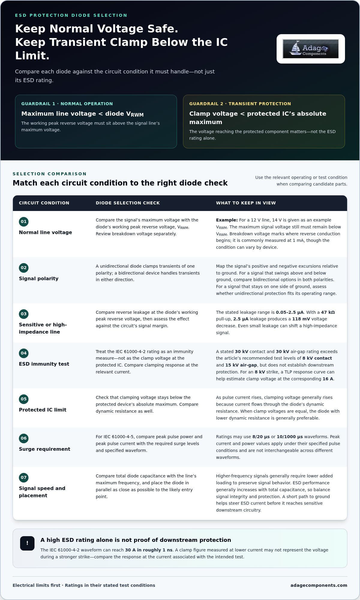
A high ESD rating alone doesn’t show whether a diode will protect a downstream IC. The key ESD protection diode clamping voltage selection criteria are to keep the diode’s working peak reverse voltage above the signal line’s maximum voltage, then confirm its clamp voltage stays below the protected device’s absolute maximum limit. Compare dynamic resistance as well: when clamp voltages are equal, the diode with lower resistance is generally preferable.
It’s easy to focus on a diode’s ESD rating, but the voltage that reaches the protected component matters just as much. This article explains how breakdown voltage, working voltage, clamping voltage, dynamic resistance, and the IC’s limits work together to guide selection.
You’ll also learn how to interpret ESD and surge ratings, account for signal-line leakage and capacitance, and assess whether a diode’s performance suits the circuit. This provides a practical framework for comparing parts against the electrical limits your design must preserve.
Key Takeaways
- Match the diode’s working voltage and polarity configuration to the signal line’s normal operating range to avoid unwanted loading or conduction.
- Account for reverse leakage on sensitive lines; even small leakage can shift a signal when the circuit uses a high-value pull-up resistor.
- Compare clamping performance under conditions relevant to the expected ESD event, not by the diode’s ESD rating alone.
- Use the protected IC’s input limits as the practical reference point, and consider how dynamic resistance affects the voltage reaching it.
- Balance protection with signal integrity by considering diode capacitance against the line’s frequency requirements.
Selecting reverse breakdown voltage or working peak reverse voltage
Keep the signal line’s maximum voltage below the diode’s working peak reverse voltage (VRWM). Then compare breakdown and clamping voltages under the conditions your circuit must withstand.
For a concise explanation of TVS devices and transient suppression, watch this overview:
Working and Breakdown Voltage
Working voltage is the highest continuous reverse voltage the diode is intended to withstand without entering avalanche breakdown. Breakdown voltage marks the point where reverse conduction begins, while clamping voltage is the voltage across the conducting diode during a transient. These values describe different operating conditions. For a 12V line, a 14V reverse working voltage is a selection example; the maximum signal voltage still must remain below VRWM.
Reverse Leakage at Working Voltage
Reverse leakage current is specified at the diode’s working peak reverse voltage, so compare leakage at that condition. The stated range is 0.05 to 2.5 μA. On a high-impedance line, that current can shift the signal: with a 47-kΩ pull-up resistor, 2.5 μA leakage produces a 118-mV voltage decrease. Assess this effect against the circuit’s signal margin.
IEC 61000-4-2 test levels describe ESD immunity, not the voltage clamped at the protected IC. A diode’s stated 30 kV contact and 30 kV air-gap rating exceeds the recommended test levels of 8 kV contact and 15 kV air-gap, but that rating alone doesn’t establish downstream protection. For an 8 kV IEC strike, a TLP response curve can help estimate clamping voltage; examine its voltage response at 16 amps, the corresponding TLP current for that test level.
IEC 61000-4-5 addresses surge requirements, so compare the diode’s peak pulse power and peak pulse current ratings with the required surge levels. Ratings may use standard waveforms such as 8/20 μs or 10/1000 μs. The waveform matters: peak current and power values apply under specified pulse conditions, and should not be treated as interchangeable across different waveforms.
As pulse current rises, clamping voltage generally rises because current flows through the diode’s dynamic resistance. The IEC 61000-4-2 waveform can reach 30 A in roughly 1 ns, making the device’s response at relevant current important. A published clamp figure at a lower current may not represent the voltage during a stronger strike; compare the response at the current associated with the intended test.
For selection, compare maximum line voltage with VRWM, then review breakdown voltage and leakage at working voltage. Check peak pulse current and power against the applicable surge waveform. Breakdown voltage is commonly measured at a specified current of 1 mA, though that condition can vary by device. These ESD protection diode clamping voltage selection criteria keep normal operation, transient response, and test conditions distinct.
How do I choose an ESD protection diode?
Start with the signal’s polarity, then match the diode configuration to its normal voltage range. Compare capacitance with the line’s maximum frequency, and check that the diode’s guaranteed ESD performance meets the system requirement.
Signal Polarity and Diode Configuration
A unidirectional diode clamps transients of one polarity, while a bidirectional device handles transients in either direction. This distinction matters when a signal can swing above and below ground. For a signal that stays on one side of ground, assess whether unidirectional protection fits its operating range. For a bipolar signal, compare bidirectional options in both polarities.
Configuration affects the diode’s behavior during normal operation as well as during an ESD event. First map the signal’s positive and negative excursions, including its reference to ground. Then compare those operating conditions with the diode’s electrical parameters and the circuit’s protection requirements. For example, an automotive signal that swings on both sides of ground needs protection for both polarities that does not interfere with normal signaling.
Capacitance and Signal Speed
Diode capacitance adds electrical load to a protected signal line, so selection depends on the line’s maximum frequency. Added capacitance can affect signal integrity, especially on faster lines. Compare the diode’s total capacitance with the interface’s frequency requirements instead of selecting by ESD rating alone.
How do capacitance and signal speed affect ESD diode selection? Choose total capacitance based on the protected line’s maximum frequency: higher-frequency signals generally require lower added loading to preserve signal behavior. ESD performance generally increases with total capacitance, so the design must balance signal integrity and protection.
Next, match the diode’s guaranteed ESD performance to the system’s immunity target. For IEC 61000-4-2 requirements, select a diode with guaranteed performance above the system requirement. The test-level rating describes the diode’s ESD capability, but doesn’t by itself establish whether the protected circuit remains within its limits. Treat the immunity rating and signal parameters as separate selection criteria.
Placement also shapes the protection path. An ESD protection diode sits in parallel with the circuit it protects and steers ESD current toward ground. Place it as close as possible to the likely entry point, such as a connector or user interface. This shortens the transient path before it reaches sensitive downstream circuitry.
For each candidate, compare polarity, operating voltage, capacitance, and guaranteed ESD performance against the design’s requirements. A unidirectional device may suit a single-polarity signal, while a bidirectional device may fit a line that swings both ways. The electronic component linecard can support sourcing decisions when your design review also includes component procurement.
Clamp voltage relative to protected-device withstand voltage
The voltage at a protected pin can exceed the diode’s clamp voltage because PCB trace inductance adds transient voltage. Read datasheet curves for the relevant pulse current and waveform, then compare the resulting clamp level with the semiconductor’s withstand limit.
Clamp Voltage and Device Withstand
Clamping voltage is the voltage across a conducting protection diode during a transient, and it matters because the protected device must withstand the voltage that reaches its pin. A lower clamp voltage generally improves protection, but the decisive comparison is with the downstream component’s absolute maximum voltage. An IEC 61000-4-2 rating describes the diode’s ESD capability, not whether the IC remains protected.
Account for the entire path between the ESD source, diode, ground, and protected pin. A long PCB trace or large current loop adds inductance, which can increase voltage during a fast current change. Place the diode close to the connector or user interface and keep its ground return short. These layout choices help reduce the extra voltage between the diode and protected device.
Check the IC’s input structure as well as its absolute maximum rating. Internal ESD diodes can turn on when an input rises above the supply voltage plus a diode’s forward voltage, or falls below ground minus that forward voltage. This conduction path does not prove the external clamp is adequate. Compare the expected pin voltage with the IC’s specified limit under the relevant operating conditions.
Datasheet Curves and Test Conditions
A clamping-voltage curve shows how the diode’s voltage changes with pulse current under stated test conditions. It matters because a single clamp figure can mislead if its current or waveform differs from the application. Read the current axis, voltage axis, pulse waveform, and test method together. TVS clamping voltage is often specified using an 8/20 μs waveform.
For example, a stated TLP result gives 8.4 volts at 1 amp. Treat that as a point on the test response, not as the clamp voltage at every current. For a different ESD level, find the curve value at the relevant current. A TLP response curve can help estimate behavior during an IEC ESD strike because its characteristics are similar to the strike.
Test conditions also explain why two datasheets may report different clamp values for similar devices. Compare measurements made at equivalent pulse currents and waveforms; don’t treat an 8/20 μs surge result as interchangeable with a fast ESD response. The diode’s dynamic resistance contributes to voltage rise as current increases, while PCB inductance adds voltage outside the device. Evaluate both effects before judging the application’s protection margin.
Use the datasheet curve to estimate the diode voltage under the intended pulse, then account for the board path to the pin. Confirm that the resulting voltage stays below the protected semiconductor’s withstand limit.
Dynamic resistance selection
Dynamic resistance describes how much a diode’s voltage rises as current increases during a transient. Compare it alongside clamping voltage: if two ESD protection diodes have the same clamp voltage, choose the one with lower dynamic resistance. Its voltage will generally rise less as current increases, reducing the voltage applied across the protected IC.
On a voltage-versus-current curve, dynamic resistance is the slope of the conducting region. In practical terms, it relates a change in current to the resulting change in diode voltage. A simplified relationship is ΔV = rd × ΔI, where rd is dynamic resistance. This explains why a diode’s clamp voltage at one current does not describe its response at every current.
Compare candidate devices at equivalent operating points. First, identify the pulse current relevant to the application. Then read each diode’s voltage at that current and examine how quickly voltage rises as current increases. A lower slope indicates lower dynamic resistance over that part of the curve. Avoid comparing values measured at different currents or under different test conditions, since they do not provide a like-for-like comparison.
Current direction matters too. For a unidirectional diode, evaluate the forward and reverse behavior relevant to the protected signal and transient polarity. For a bidirectional device, examine its response in both directions. A single curve may show only one polarity or operating region, so confirm that the data covers the direction the circuit must withstand.
Consider the full voltage path. During conduction, the diode’s voltage appears across the protected circuit, and its dynamic resistance contributes to the voltage increase as pulse current rises. Board layout can add further voltage at the IC pin, so the datasheet clamp value is not necessarily the maximum pin voltage. Keep the diode close to the transient entry point and minimize its connection to ground.
Dynamic resistance helps distinguish devices when their headline clamp ratings are similar. For example, if two candidates have the same stated clamp voltage, compare their voltage-current curves around the application’s expected pulse current. Prefer the flatter conducting curve, provided the diode also meets the required working voltage, polarity, and ESD performance. This makes the comparison specific to the actual operating range rather than a single maximum rating.
Use datasheet values consistently: compare the same test method, pulse condition, and current direction. Then assess the resulting diode voltage against the protected component’s absolute maximum limit. Lower dynamic resistance can reduce the extra voltage developed as current increases, but you still need to consider clamp level, layout, and device withstand limit together.
Clamping voltage and protected-component limits
The decisive check is whether the voltage reaching the protected component stays below its absolute maximum limit. A diode’s ESD rating describes the stress it can withstand, not the protection margin at a downstream pin.
Start with the protected IC’s input limits, then compare them with the diode’s clamping voltage under relevant pulse conditions. A lower clamp voltage generally provides better ESD protection. But choose a diode whose voltage at the expected pulse current is compatible with the device’s limit, not simply the one with the lowest headline rating.
For example, a TLP result gives a clamping voltage of 8.4 volts at 1 amp. Treat this as one measured point, not a universal value for every pulse. Compare that point with the IC’s specified withstand limit, then examine the diode’s response at other relevant currents. A clamp value measured at one current cannot establish protection at a higher current.
The complete path matters. A conducting diode’s voltage appears across the protected circuit, while PCB trace inductance can add voltage between the diode and IC pin during a fast transient. Place the protection device close to the entry point and keep its path to ground short. This reduces the extra voltage the layout can add at the component.
Also account for the IC’s internal protection. Its ESD diodes can turn on when an input rises above the supply voltage plus a diode’s forward voltage, or falls below ground minus that forward voltage. This internal path does not replace comparing external clamp voltage with the IC’s absolute maximum limit. Review both signal polarities and supply conditions.
Read the test conditions beside each datasheet curve. TVS clamping voltage is often specified with an 8/20 μs waveform, while ESD testing uses a different transient profile. Compare voltage and current under conditions relevant to the application. The IEC 61000-4-2 rating indicates what the diode itself can withstand; it does not prove the downstream semiconductor stays within limits.
For consumer electronics or industrial equipment, document the comparison using the IC limit, diode voltage at the relevant pulse current, and test waveform. Include layout effects rather than treating the datasheet clamp figure as the pin voltage. Together, these characteristics determine whether the protection choice fits the circuit’s actual withstand boundary.
Use the electronic components linecard to support component evaluation alongside your protection design review.
Adage Components: Thick Film Chip Resistors
Adage Components supports component sourcing alongside your ESD-protected design, with Thick Film Chip Resistors, Thin Film Precision Resistors, and Carbon Film Resistors. We offer manufacturer pricing and OEM pricing, with one of the best costs in the industry and the same advantages as buying from tier 1 distributors at OEM pricing.
We source authentic components through vetted manufacturers and partner suppliers, many franchised by top 100 distributors. Our international logistics program supports short lead times and integration with your MRP system, helping coordinate delivery to your facility in real time, on time.
Contact Adage Components to discuss your resistor sourcing needs.
Carry Your Protection Decision Into Procurement
Once engineering has defined acceptable protection limits, carry those requirements into component selection and procurement planning. Record the relevant electrical parameters for each candidate part so future reviews can assess substitutions against the same design constraints. This creates a clearer handoff between circuit design and purchasing, especially when a component changes during a product’s lifecycle.
Use the ESD protection diode clamping voltage selection criteria as part of the decision record, not as a standalone rating check. Keep the selected device aligned with the protected component’s limits and the application’s operating conditions. A disciplined review helps procurement teams compare suitable parts without losing sight of circuit requirements.
For your next component review, explore Adage Components’ linecard and identify parts relevant to your sourcing requirements. A well-documented selection gives your team a practical foundation for the next design and procurement decision.
Frequently Asked Questions
What is Clamping Voltage in TVS Diodes?
Clamping voltage is the voltage across a TVS diode while it conducts transient current. It varies with current and pulse conditions, so a datasheet value describes a specific test point, not every ESD event. Compare the listed voltage at the pulse current relevant to your design. This distinguishes a device’s clamp performance from its working or breakdown voltage.
What is ESD diode clamping voltage and how is it measured?
Clamping voltage is the voltage across an ESD diode during a discharge or simulated pulse. A test applies a defined current waveform and measures the diode’s voltage response. The reported value is meaningful only alongside those test conditions. For a useful comparison, match the test method, waveform, and current across candidate datasheets. A voltage measured under one pulse condition should not be assumed to apply under another.
How to compare ESD diode clamping voltage with an IC’s absolute maximum voltage?
Compare the IC’s absolute maximum input limit with the voltage expected at its pin during a transient, considering both polarities. The diode’s terminal voltage may differ from the pin voltage because board connections affect the transient path. For example, check whether a positive strike could push an input beyond its upper limit, then assess negative stress against its lower limit. Keep normal signal excursions within operating conditions as well.
How to choose an ESD diode clamping voltage for USB, HDMI, Ethernet, and other interfaces?
Start with the specific interface version and signal type, then compare its normal voltage range, maximum signal frequency, and required ESD immunity. USB, HDMI, and Ethernet designs can have different channel and signal-integrity constraints, so don’t select by interface name alone. Review capacitance and relevant protection data for the exact line. For multi-line ports, assess each protected signal path and its connection to ground.
What are the risks of choosing an ESD diode with clamping voltage that is too high or too low?
A clamp voltage that is too high can leave the protected IC exposed to voltage beyond its withstand limit during a transient. A voltage that is too low can cause conduction or loading during normal signal operation if it conflicts with the line’s operating range. This may distort the signal or increase leakage effects. Compare operating conditions and transient behavior together instead of choosing solely for the lowest clamp figure.
Disclaimer
Cross-referenced components needs to be confirmed by the client with either spec. sheet or samples or both.
Please note, we use AI to help us, information is verified to be correct but we can not guarantee 100% accuracy.