

A current-sense resistor can add switching noise to the signal it is meant to measure. Its parasitic inductance produces an L·di/dt voltage in addition to the resistor’s voltage drop. Fast current changes can therefore create spikes or ringing, distorting the sensed value and affecting control. The impact of current sense resistor parasitic inductance on switching noise depends on the resistor, its connections, and the current-sense loop layout.
A low-inductance part can help, but component choice alone will not fix a noisy measurement. Kelvin connections, shunt placement, and the area enclosed by the sense loop all affect how much switching noise reaches the controller.
This article explains how resistor ESL creates measurement error, why four-terminal sensing and careful trace routing matter, and how placement differs in buck, boost, and buck-boost converters. It also shows how to weigh noise and accuracy against efficiency and component cost when selecting a current-sensing approach.
Key Takeaways
- Use Kelvin connections to separate the measurement path from current-carrying resistance and reduce errors from traces and solder joints.
- Choose shunt placement based on the converter topology and the current signal the controller needs to measure.
- Keep the sense loop compact and its traces routed away from noisy switching nodes to limit inductive pickup.
- Evaluate resistor ESL alongside resistance, power loss, accuracy, and control-loop response when selecting a current-sensing component.
- Match resistor construction to the design’s precision and sourcing requirements; Adage Components offers several resistor categories for different applications.
Kelvin and four-terminal shunt connections
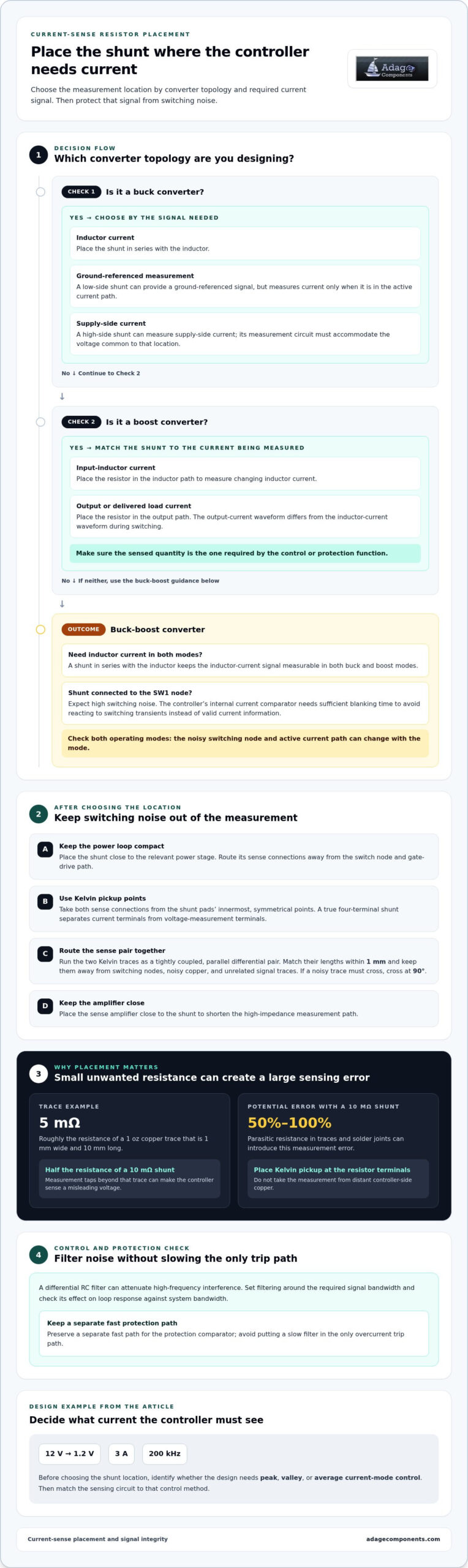
Kelvin sensing takes the voltage measurement from separate points on the shunt, rather than through the current-carrying connections. This matters because the wanted signal across a low-value resistor can be comparable to unwanted voltage drops in copper, solder, and wiring. With a 10 mΩ shunt, parasitic resistance in traces and solder joints can introduce a 50% to 100% measurement error.
A true four-terminal shunt separates its current terminals from its voltage-measurement terminals. This arrangement excludes solder-joint resistance from the measurement, but PCB routing still matters. Kelvin sensing is also used with inductor-DCR sensing, since both methods produce small signals that can be overwhelmed by noise pickup.
Long wires and poorly placed traces can couple switching interference through stray capacitance and mutual inductance. Place the sense amplifier close to the shunt to shorten the high-impedance measurement path. Take both sense connections from the shunt pads’ innermost, symmetrical points to exclude voltage drops along the current path.
Route the two Kelvin traces together as a tightly coupled, parallel differential pair. Match their lengths within 1 mm and keep them away from switching nodes, noisy copper, and unrelated signal traces. If a noisy trace must cross the pair, cross it at 90 degrees to reduce inductive coupling. A described Kelvin-trace layout with a shield plane reduced common-mode coupling by more than 15 dB.
Trace resistance can undermine an otherwise accurate shunt. For example, a 1 oz copper trace that is 1 mm wide and 10 mm long has roughly 5 mΩ resistance. That is half the resistance of a 10 mΩ shunt, so placing measurement taps beyond that trace can make the controller sense a misleading voltage. The Kelvin pickup points should sit at the resistor terminals, not at distant controller-side copper.
To reduce switching noise without slowing protection, filter the measurement or control path while preserving a separate fast path for the protection comparator. A differential RC filter can help attenuate high-frequency interference, but its effect on loop response should be checked against the system’s bandwidth. Set filtering around the required signal bandwidth, and avoid placing a slow filter in the only overcurrent trip path.
These layout choices address different sources of error: four-terminal construction limits terminal-resistance effects, while paired Kelvin routing reduces coupled noise. Together, they help the shunt signal represent actual current before it reaches the amplifier or controller.
Sense resistor placement in buck, boost, and buck-boost converters
Place the shunt where it measures the current signal the controller uses, while keeping its power connections separate from the sensitive measurement path. To reduce switching-noise pickup, keep the resistor close to the relevant power stage and route its sense connections away from the switch node. The right position depends on converter topology and whether control requires input, output, or inductor current.
In a buck converter, a shunt in series with the inductor measures inductor current, which changes as the switching stage transfers energy. A low-side shunt can provide a ground-referenced signal, but measures current only when it lies in the active current path. A high-side shunt can measure supply-side current, but its measurement circuit must accommodate the voltage common to that location.
In a boost converter, identify whether the design needs input-inductor current or output current before choosing the shunt position. A resistor in the inductor path measures changing inductor current; one in the output path measures delivered load current. These waveforms differ during switching, so the sense signal must represent the quantity used by the control or protection function.
A buck-boost converter adds a mode-change complication. Placing the resistor in series with the inductor keeps the inductor-current signal measurable in both buck and boost modes. By contrast, a shunt connected to the SW1 node faces high switching noise. The controller’s internal current comparator therefore needs sufficient blanking time to avoid responding to switching transients instead of valid current information.
Consider a 12 V to 1.2 V converter delivering 3 A at 200 kHz. Before choosing a shunt location, identify whether the design needs peak, valley, or average current-mode control. A resistor in series with the inductor can support all three approaches, but the sensing circuit must match the chosen control method. Switching-node proximity and parasitic resistance or inductance can distort the measured waveform.
Keep the shunt’s power loop compact, and avoid routing its measurement connections beside the SW node or gate-drive path. Rapid voltage transitions at the switch node can couple into nearby conductors, while long connections can add parasitic resistance and inductance. In a buck-boost design, check both operating modes because the noisy switching node and active current path can change with the mode.
Use the measured current requirement to guide component selection, then assess the resistor’s electrical characteristics alongside its board position. Comparing resistor component options can help align the selected part with the converter’s sensing role and layout constraints.
Sense-loop area and inductive voltage spikes
A sense loop converts changing current into a voltage that can resemble a real change in load current. The measured signal includes both the resistor’s voltage drop and an inductive term: Vsense = I × R + L × di/dt. The faster the current changes, the greater the inductive contribution. A larger loop area also increases susceptibility to magnetic coupling from nearby power paths.
Long wires add parasitic inductance, so their voltage disturbance rises during rapid current transitions. One reported example linked a 12 nH wire-wound sense resistor with a current loop that shut down every few seconds. The resistor value alone therefore doesn’t define measurement quality. Lead geometry, connection length, loop area, and switching-edge speed all influence the signal delivered to the controller.
To limit induced spikes, keep the outgoing and return sense paths close together. Their opposing magnetic fields reduce the loop’s response to external flux. Route the pair away from the switch node, gate-drive traces, and high-current commutation loop. If the measurement connection must cross a noisy path, minimize the shared parallel length and avoid routing the sense loop around large areas of copper.
An oscilloscope can help distinguish an inductive artifact from the underlying current signal. Compare the spike’s timing and shape with switching transitions: a narrow transient synchronized with a fast edge suggests coupling or the L × di/dt term, while a current-related signal should follow the expected circuit current ramp. Measure across the shunt with a low-inductance probe connection, and compare the result with the switch-node waveform when practical.
Probe setup matters. First short the oscilloscope probe signal to its ground while disconnected from the circuit; this reveals noise generated by the probe and instrument. Then inspect the measured waveform using suitable channel bandwidth. A reported test used a 20 MHz oscilloscope channel, while a separate low-frequency oscillator measurement needed around 10 kHz of bandwidth. Those settings serve different measurement goals, so bandwidth should match the transient being investigated.
Do not treat a filtered trace as proof that a spike has disappeared. A low-pass filter can suppress high-frequency content on the display, but its bandwidth may also hide real current changes. Compare filtered and unfiltered measurements, and retain a fast protection path when filtering the control signal. This helps distinguish measurement cleanup from a genuine change in circuit behavior.
A compact sense loop improves signal integrity and makes troubleshooting easier. If a converter shows unexplained shutdowns or current spikes, inspect the shunt connections and probe loop before changing control thresholds. The measured voltage reflects the current-sensing resistor’s resistance, parasitic inductance, and layout together, not resistance alone.
Current sensing accuracy, efficiency, and cost
Current-sense design balances signal strength against power dissipation. A smaller resistance reduces the shunt’s voltage drop and I²R loss, but also produces a smaller signal for the amplifier. For example, a 1 mΩ shunt carrying 100 A produces a 100 mV signal. That value supports measurement, but circuit noise and offset consume a larger share of the available signal.
Increasing resistance makes the measured voltage easier to distinguish, but raises dissipation at the same current. A useful comparison is the 10 mΩ example carrying a 5.3 A current amplitude, which produces a 0.053 V peak-to-peak voltage drop. Designers must assess this signal against the allowable power loss and thermal rise, not optimize measurement amplitude alone.
Accuracy also depends on resistance stability. Sense resistors can have a temperature coefficient on the order of 100 ppm/°C. By comparison, an ordinary thick-film resistor rated at 200 ppm/°C can drift 1.2% after a 60 °C temperature rise. That change directly affects the current calculated from voltage divided by resistance, even when the measurement electronics remain stable.
System-level sensing error depends on the method and operating conditions. Sense-resistor current sensing typically has an error between 1% and 5%. MOSFET RDS(ON) sensing avoids a separate series shunt, but RDS(ON) values can vary by 33% or more. Its temperature coefficient can exceed 80% over 100 °C, making it comparatively inaccurate as temperature changes.
Efficiency comparisons should account for both conduction loss and the effects of inaccurate current information. A shunt’s power loss follows I²R, so resistance selection matters especially at high current. Lower resistance can reduce that loss, but the smaller signal may require more careful amplification and filtering. The decision therefore involves the power path, sensing circuit, and control response.
Cost means more than the shunt’s purchase price. A component with suitable stability and low parasitic effects can support dependable control, while inadequate accuracy may require design changes or tighter calibration. Compare candidate parts by resistance tolerance, temperature behavior, power handling, and parasitic inductance. Then assess the complete sensing implementation, including amplifier and layout requirements.
For procurement, match the component specification to the required accuracy and thermal operating range. A precision design may prioritize stable resistance, while a loss-sensitive power stage may favor lower resistance. Review the current waveform alongside the error budget. This clarifies whether the design needs a stronger signal, lower dissipation, or tighter resistance stability.
Sense-resistor ESL can cause significant ringing on the switch gate driver and add ripple to the current-sense signal, degrading current-sensing accuracy. A low-inductance 0.4 nH sense resistor reduced phase error from 2.7° to 0.11° and raised loop crossover from 8 kHz to 12 kHz. Sense resistors typically cost between $0.05 and $0.20.
Sense resistor ESL and switching noise
Resistor ESL adds an inductive voltage to the resistive signal during fast current changes. The resulting ripple or spike can distort measurements and affect control-loop behavior. To understand the impact of parasitic inductance in a current-sense resistor on switching noise, consider the resistor’s construction, the current ramp, and the connections.
Inductance Across Resistor Constructions
Current-sense resistor inductance depends on the element and terminal geometry, not just resistance value. Metal-strip designs can have ESL below 1 nH, while a wire-wound example measured 12 nH. Metal-foil construction can also support low inductance, but its performance depends on the current path and connection layout.
This difference matters because parasitic inductance changes the sensed waveform. Lead inductance can introduce phase error, so account for it when evaluating current-sense signals. Compare construction data with the mounted circuit, since PCB connections contribute to total inductance.
Voltage Spikes at a Given Current Change
The inductive voltage spike follows V = L × di/dt, so faster current ramps or greater ESL produce larger errors. For a 10 mΩ shunt with 10 nH ESL, an example produced 0.106 V during a 0.5 μs current ramp, and -0.0118 V during a 4.5 μs ramp.
These examples show why resistance alone cannot predict the measured signal. A high-frequency transient can exceed the shunt’s resistive voltage, making the controller interpret a switching edge as a current change. The impact of parasitic inductance in a current-sense resistor on switching noise therefore depends on both ESL and di/dt.
Package Size and Construction Effects
Package geometry affects the length and arrangement of current paths, which shape ESL. Low-profile surface-mount plate structures include 0805, 1206, 2010, and 2512 sizes; reverse-geometry 0612 and 1225 parts are identified as better choices for minimizing ESL.
For high-frequency sensing, compare the resistor structure and its mounted connections. A metal-strip shunt with ESL below 1 nH can reduce inductive error, while longer leads add parasitic inductance. This is a practical factor in the current-sense resistor parasitic inductance impact on switching noise.
ESL also affects regulator accuracy and stability. Shunt parasitic inductance reduces gain at higher frequencies, while ripple on the sense signal can shift control-loop behavior. In a 500 kHz SiC ringing band, a 3 nH lead produced more than 25° of phase error. A low-ESL resistor changed measured phase margin from 32° to 58° and reduced overshoot from 28% to 6%.
An inductive spike that crosses the comparator threshold can trigger a false overcurrent trip or delay detection. Distorted feedback can also affect switching losses through the controller’s response. Select ESL with the protection and control bandwidth in mind, then validate the waveform in the assembled circuit.
To compare resistor constructions for current sensing, review the current-sensing resistor options and match the component structure to the required ESL and layout.
Adage Components: Thick Film Chip Resistors
Adage Components offers Thick Film Chip Resistors and helps OEMs source authentic components through vetted manufacturers and partner suppliers, many franchised by top 100 distributors. We offer manufacturer pricing and OEM pricing, with the same advantages as buying from tier 1 distributors but at OEM pricing, alongside one of the best costs in the industry.
Our sourcing supports commercial and automotive grade components, with compliance across ISO certifications. An international logistics program and growing state-of-the-art warehouse support short lead times and MRP integration, helping products reach your facility in real time, on time. Thin Film Precision Resistors and Carbon Film Resistors are also available for different component requirements.
Contact Adage Components to discuss resistor options for your sourcing needs.
Make the next design decision with confidence
Before releasing a current-sensing design, treat the measurement path as part of the power-stage design, not as an isolated component choice. Assessing the impact of current-sense resistor parasitic inductance on switching noise helps focus validation on the resistor, its connections, and the control response together. Test the assembled circuit to confirm that the sensed waveform supports the required accuracy and protection behavior.
Then align component selection with the design’s electrical requirements and procurement priorities. Adage Components offers Thick Film Chip Resistors, Thin Film Precision Resistors, and Carbon Film Resistors for consideration across resistor applications. Match the part to your design criteria and sourcing needs before finalizing the bill of materials.
Explore resistor options with Adage Components for your next current-sensing design. A disciplined review now can help your team move forward with a more informed component decision.
Frequently Asked Questions
How does parasitic inductance in a current-sense resistor create switching noise?
Parasitic inductance generates voltage whenever current changes, adding an unwanted component to the resistor’s sensed voltage. Because switching edges cause rapid current changes, this voltage can appear as spikes or ringing and may trigger a comparator even when average current remains below its threshold. Compare the sense waveform with the switching edge: a disturbance aligned with that edge may indicate inductive error rather than a genuine increase in load current.
What are typical parasitic inductance values for current-sense resistors?
There isn’t one value that applies across all current-sense resistors; construction, terminals, and PCB connections affect total inductance. Examples include a low-inductance 0.4 nH resistor, a 3 nH lead, and a 12 nH wire-wound resistor. Metal-strip parts are described as usually below 1 nH. Treat these as design examples, not a universal range, and assess the mounted component and its connections in your circuit.
How can Kelvin connections reduce switching noise in current-sense resistor measurements?
Kelvin connections give the measurement amplifier separate voltage-sense points, helping it measure the shunt signal without including as much voltage from the power connections. They also provide a defined differential path for the signal. For example, in a compact converter with noisy switch-node copper, route the pair away from that node and avoid a long shared parallel path. Kelvin routing reduces pickup, but cannot remove inductance within the resistor itself.
Disclaimer
Cross-referenced components needs to be confirmed by the client with either spec. sheet or samples or both.
Please note, we use AI to help us, information is verified to be correct but we can not guarantee 100% accuracy.